5 things to know about PCB footprints
.jpg)
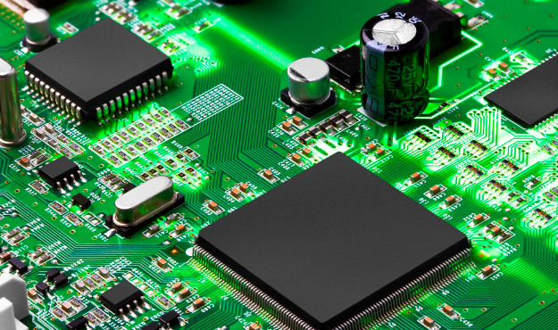
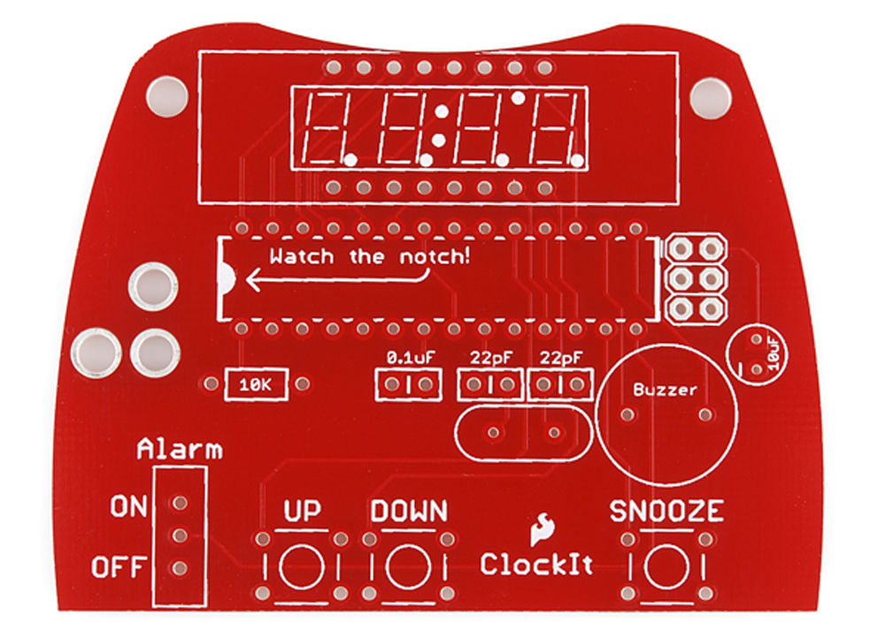
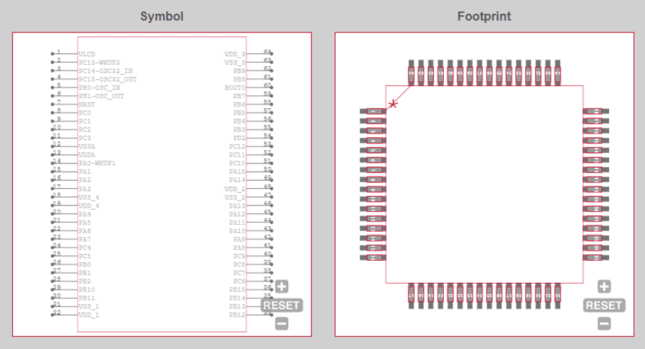
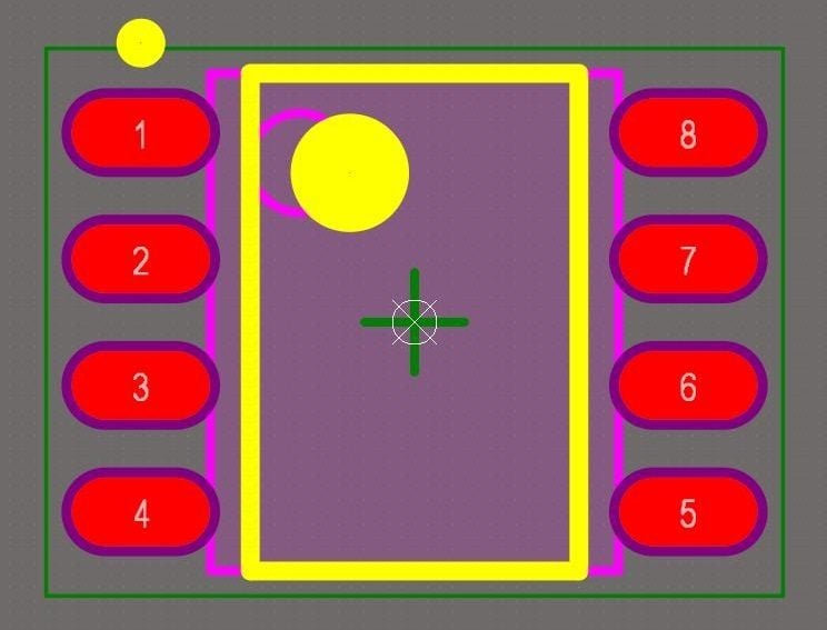
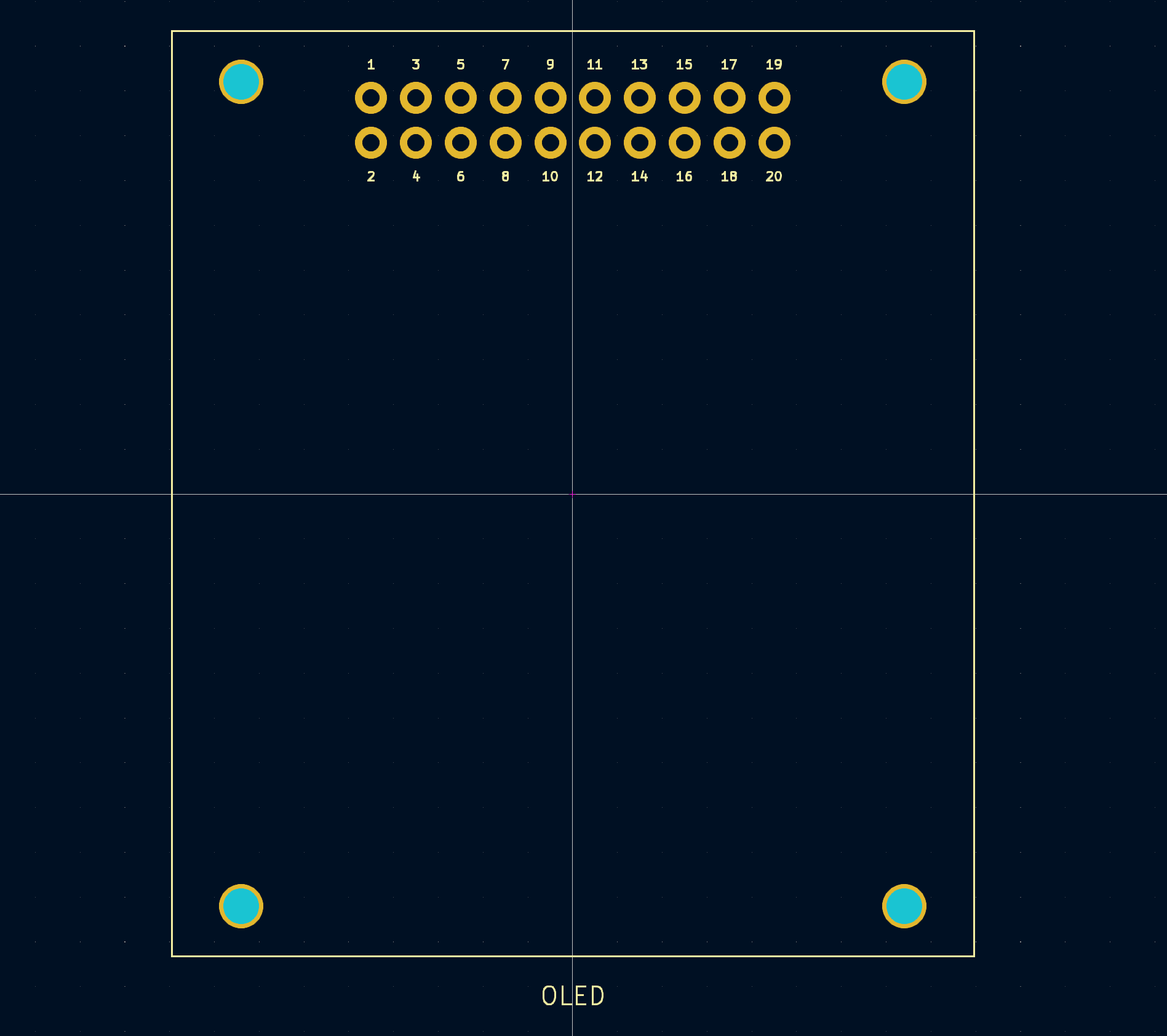
Each component placed on the sides of a printed circuit board must have its own footprint.
Best Practices for Designing a PCB Layout - Circuit Basics
How to Estimate the Board Space Required for the Components in

How can i assign a footprint to a symbol? - FAQ - KiCad.info Forums
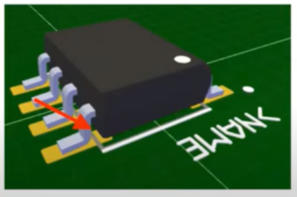
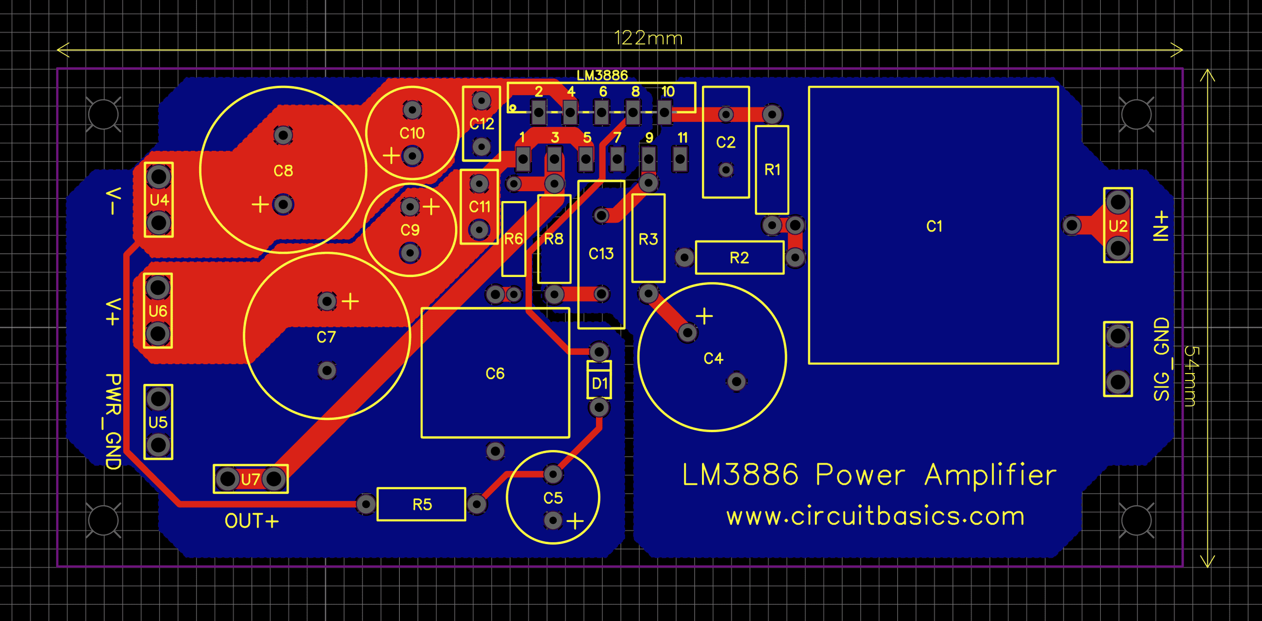
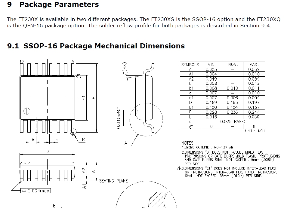
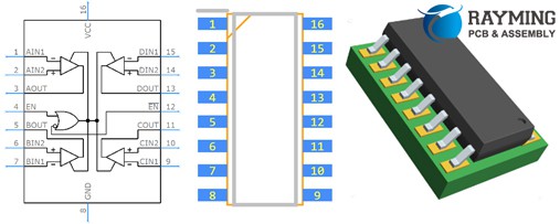
How to Design Correct PCB Footprints
PCB Basics - SparkFun Learn
Free PCB Footprints and Schematic Symbols for Designers to Use
5 things to know about PCB footprints
Designing PCBs: SMD Footprints - SparkFun Learn
Three Ways to Hack a Printed Circuit Board - IEEE Spectrum

Create a Footprint using IPC Compliant Footprint Wizard - Part 1
Designing your own PCBs - lcamtuf's thing
The Difference between Footprints and Land Patterns in PCB - RAYPCB

What is the difference between footprints and symbols? - FAQ
How to Design Correct PCB Footprints


/cdn.vox-cdn.com/uploads/chorus_asset/file/13064221/newlede1_2040.0.0.1443461562.jpg)