BGA X-Ray Good/Bad voids - Electrical Engineering Stack Exchange

Proper inspection strategy

Electronic module assembly - ScienceDirect

Interconnect Quality and Reliability of 3D Packaging
The Factory Floor « bunnie's blog

Bulletin Daily Paper 08-11-15 by Western Communications, Inc. - Issuu

Page 182 – RAYPCB

Interconnect Quality and Reliability of 3D Packaging
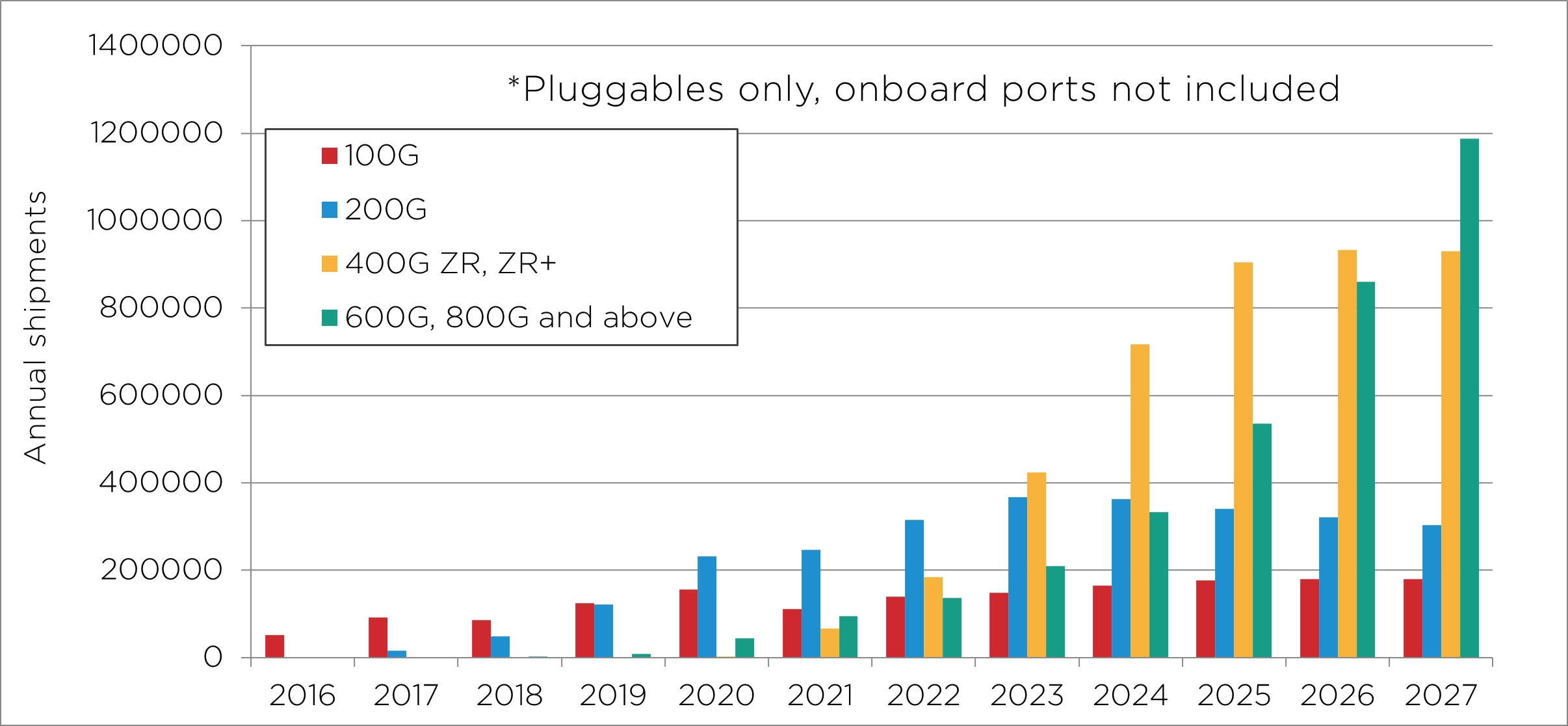
Insights - EFFECT Photonics
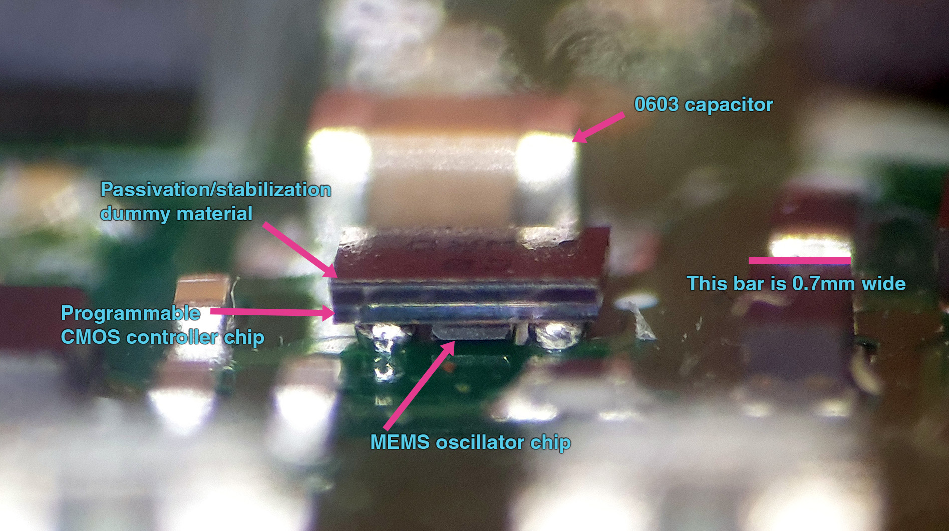
The Factory Floor « bunnie's blog

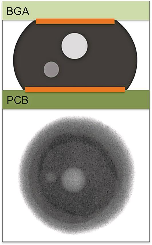
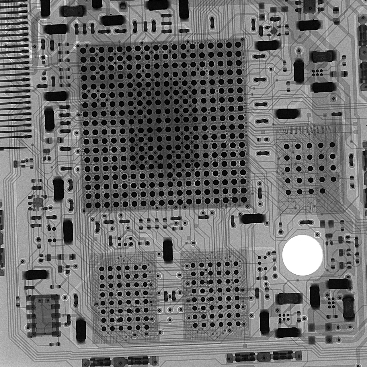
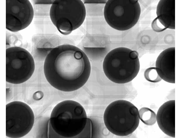
X-ray of a BGA with many large voids. The microvias can be seen at the
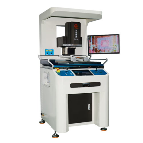
3D X-Ray Inspection (AXI) of PCBs - GÖPEL electronic

X-Ray Tips and Tricks: BGA Inspection
Eterbase Coin (XBASE) Overview - Charts, Markets, News, Discussion and Converter


Proposer des recherches