HBM PHY Cadence

Understanding ESD HBM in IC Design - AnySilicon
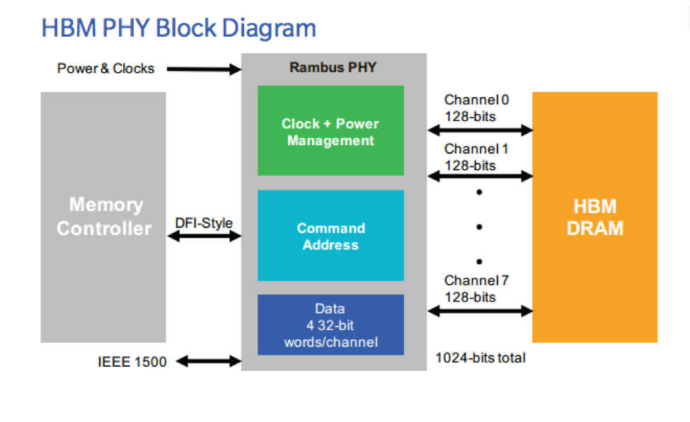
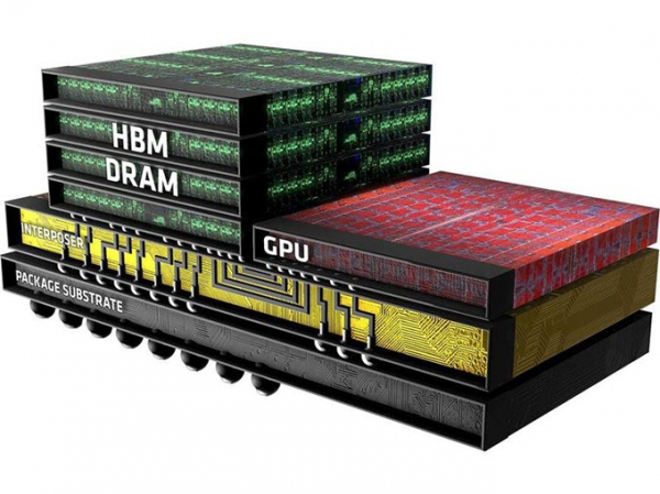
Taking a closer look at Rambus' HBM GEN2 PHY - The Next Platform

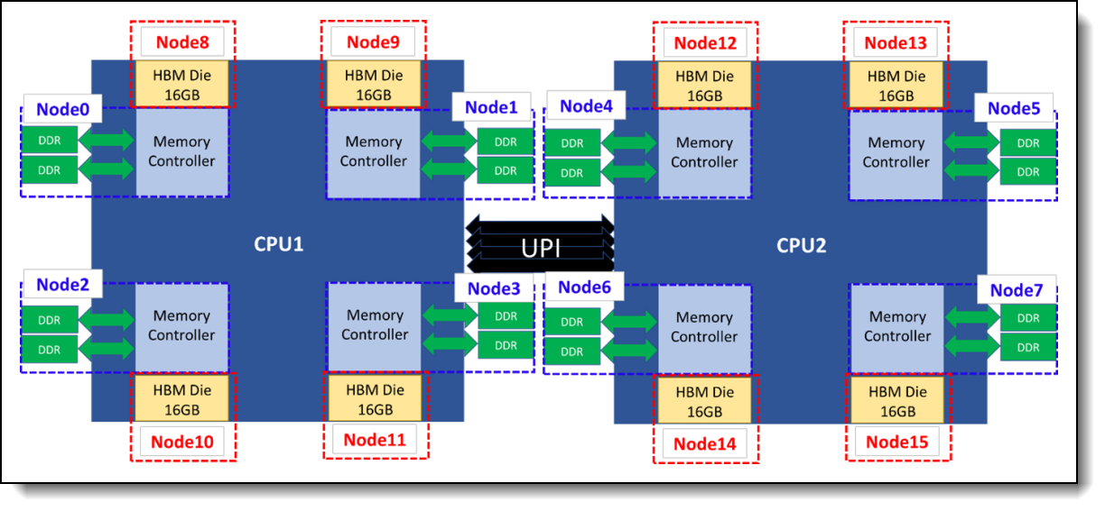
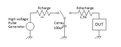
Diagram for the three blocks implemented in Cadence SPICE to carry out

AI SoC Chats: Memory Interface IP - DDR, LPDDR, HBM, GDDR

HBM2 PHY for Samsung IP Core

SK hynix DRAM Product Planning Spearheads the Memory Evolution in the Post-HBM3 Era - EE Times

Ethernet 16G Multi-protocol PHY

Cadence to Acquire Rambus PHY IP Assets - Rambus

AMD Working With Hynix For Development of High-Bandwidth 3D Stacked Memory

Rambus sells its PHY business to Cadence

HBM Controller IP - Rambus
Diagram for the three blocks implemented in Cadence SPICE to carry out

High Bandwidth Memory (HBM2) IP Subsystem Solution for 2.5D HBM ASIC SiPs — Alphawave Semi Technical Article
High-Bandwidth Memory (HBM) - Semiconductor Engineering