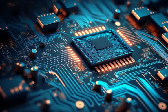
PCB Technologies - PCB Fabrication, PCB Design, IC Packaging
All-in-One PCB Solutions Provider of Miniaturization & Advanced IC Packaging Solutions, PCB Fabrication & Full Turnkey PCBA Services.
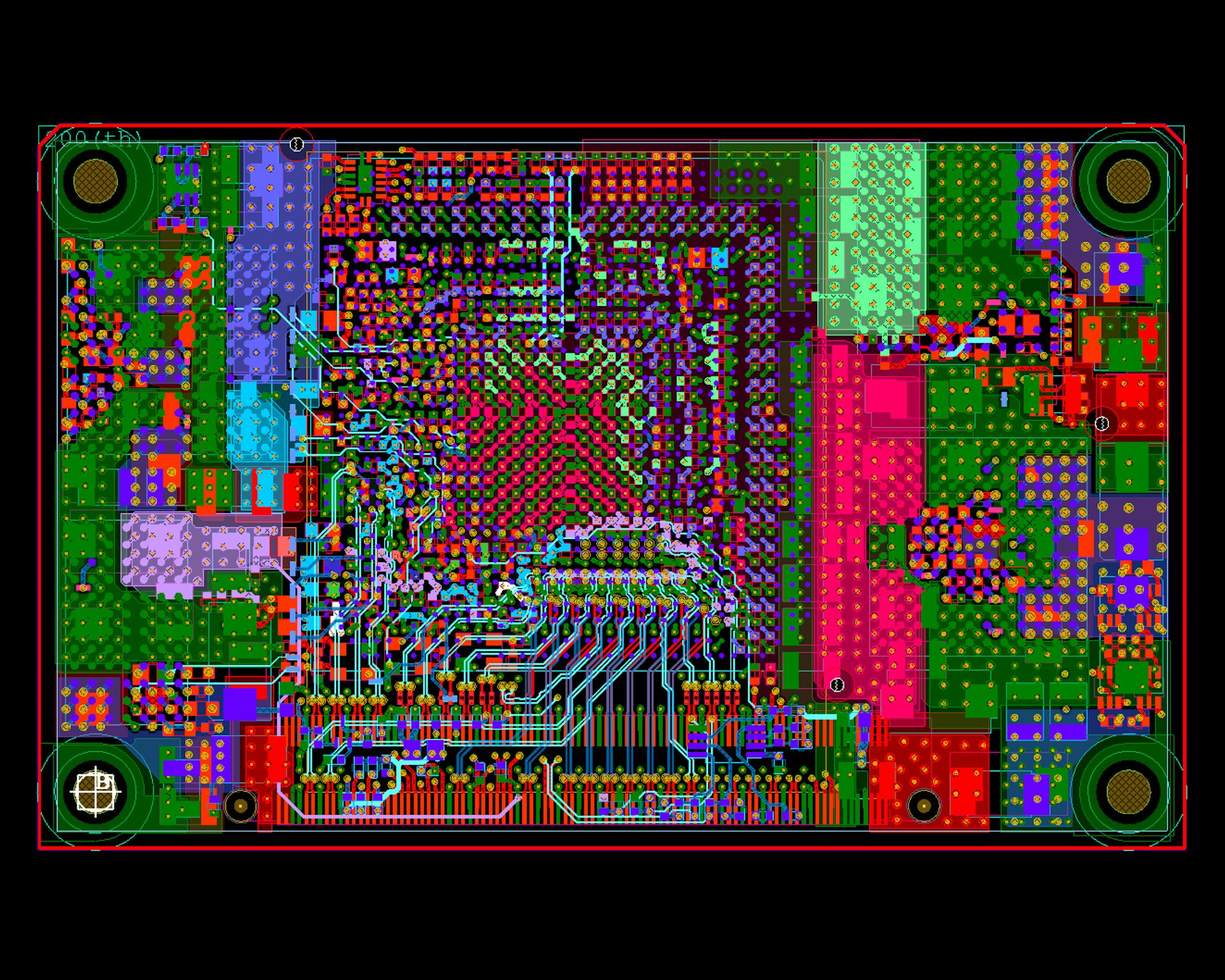
Simulation for Printed Circuit Board Design Reliability

Step by Step to Explain Printed Circuit Board (PCB) Manufacturing Process - RAYPCB

Sustainable Additive Manufacturing of Printed Circuit Boards - ScienceDirect
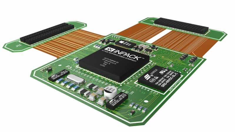
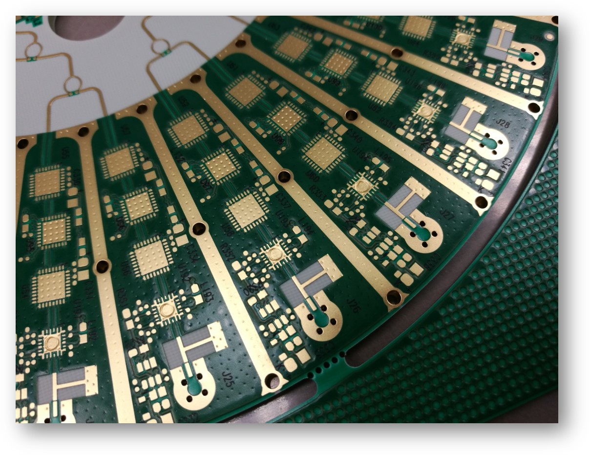
PCB design solutions
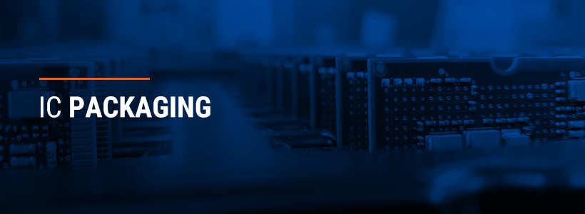
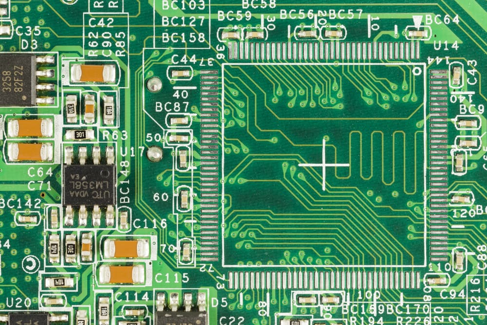
What Is IC Packaging & Why Is It Important?
Resources - PCB Fabrication, PCB Design, IC Packaging

Resources - PCB Fabrication, PCB Design, IC Packaging
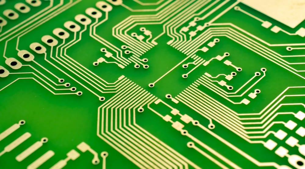
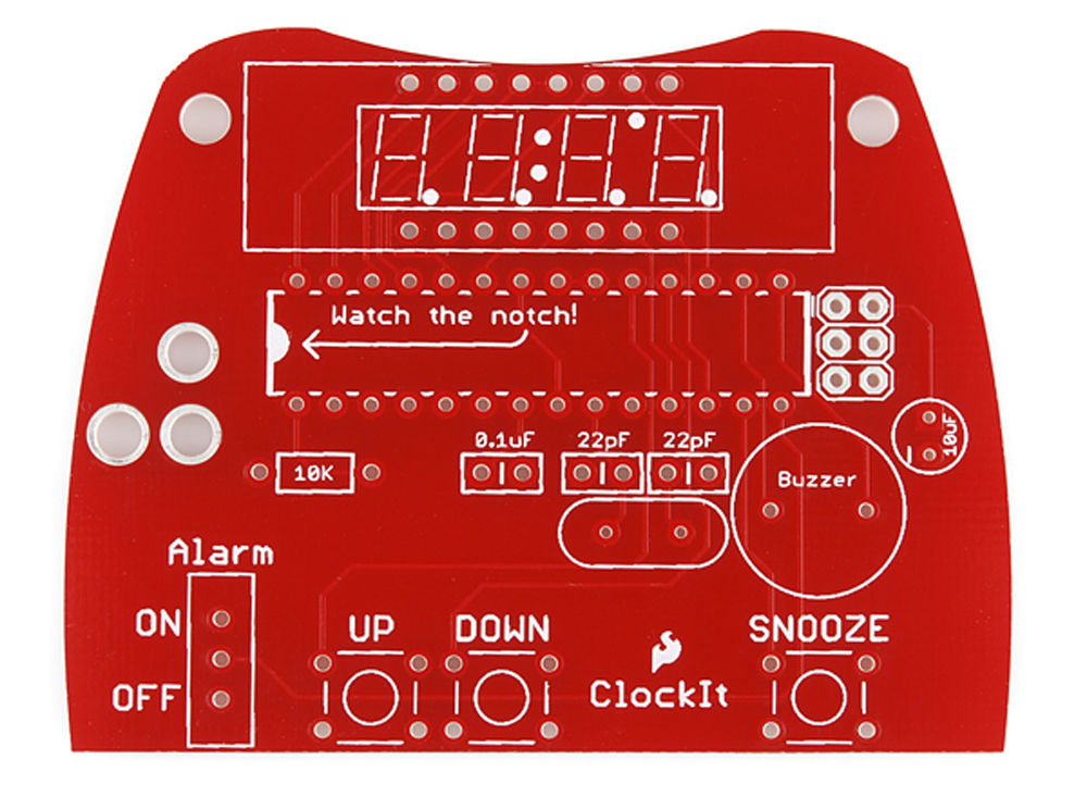
Trace PCB: A Comprehensive Guide
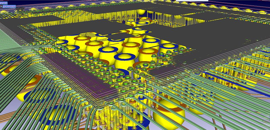
3D Multi-board Product-level PCB/IC Packaging Design - Zuken Blog
How to Design a PCB Layout: A Comprehensive Guide
Tu pourrais aussi aimer