Trace PCB: A Comprehensive Guide
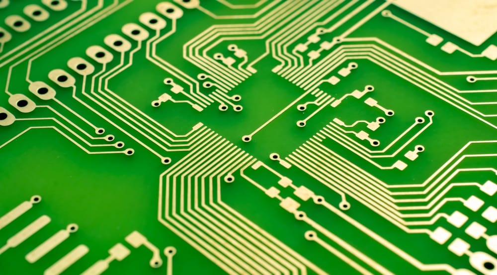
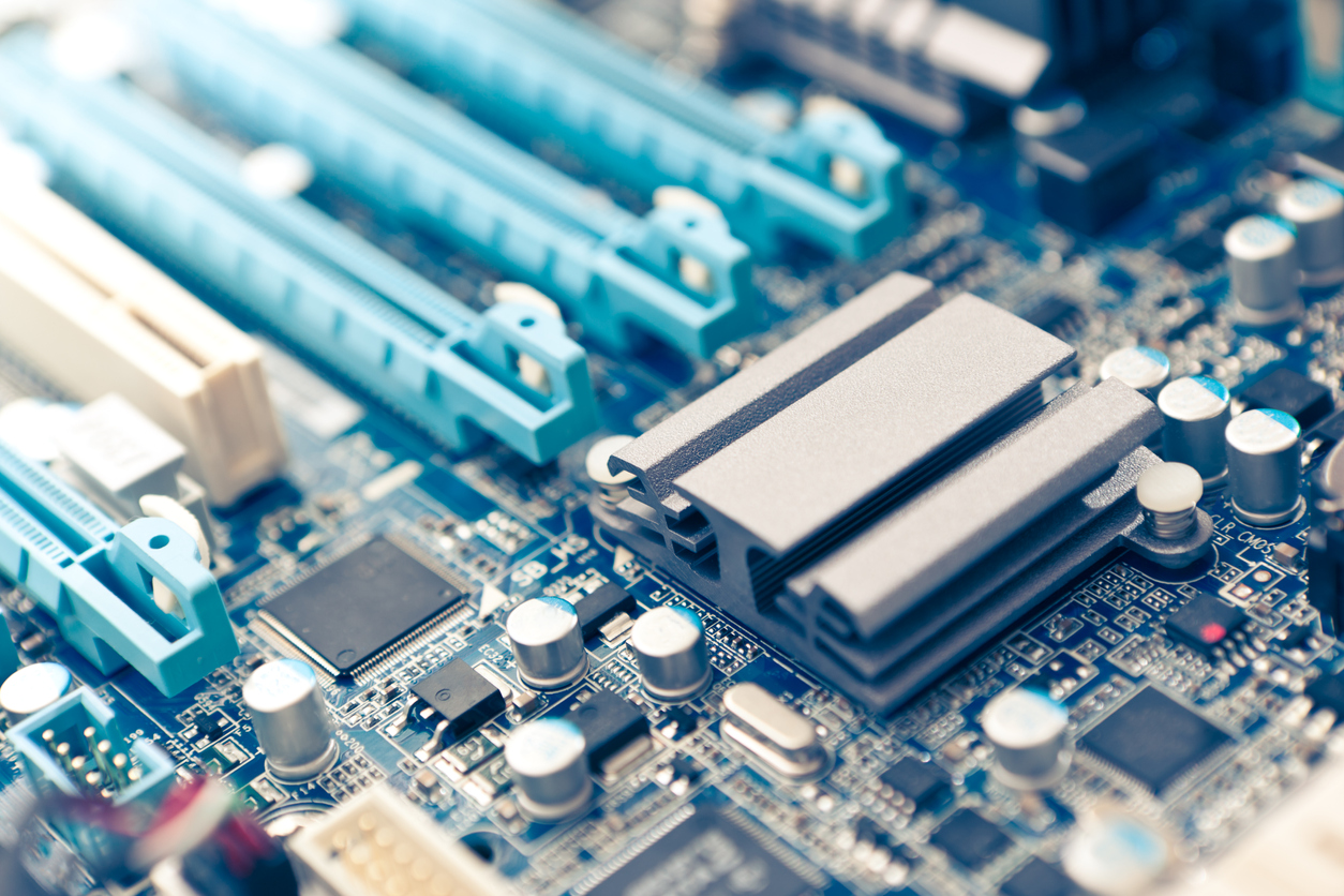
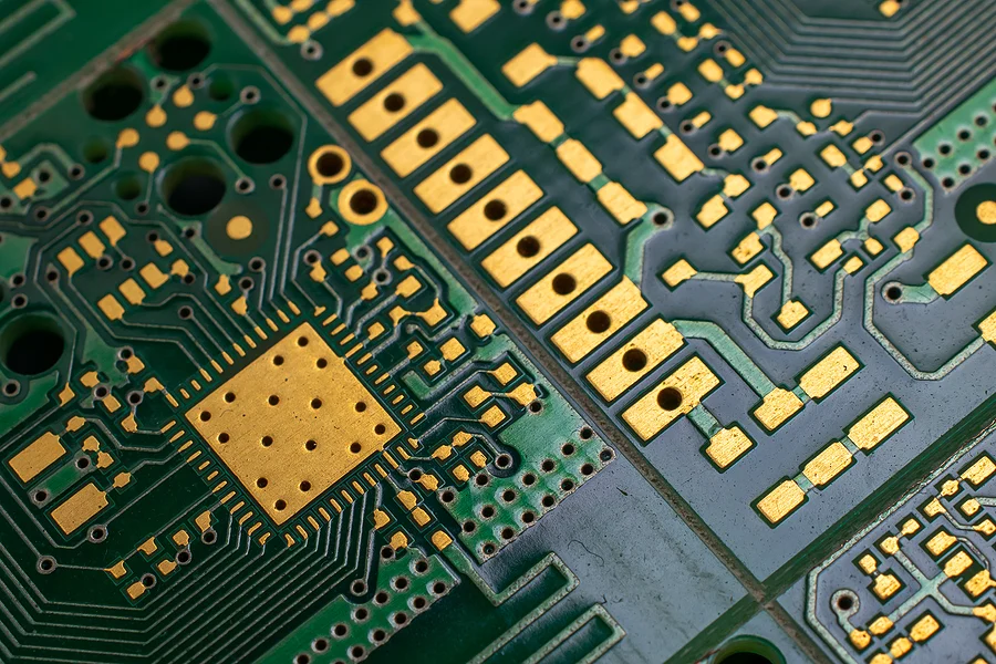
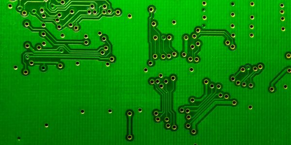
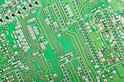
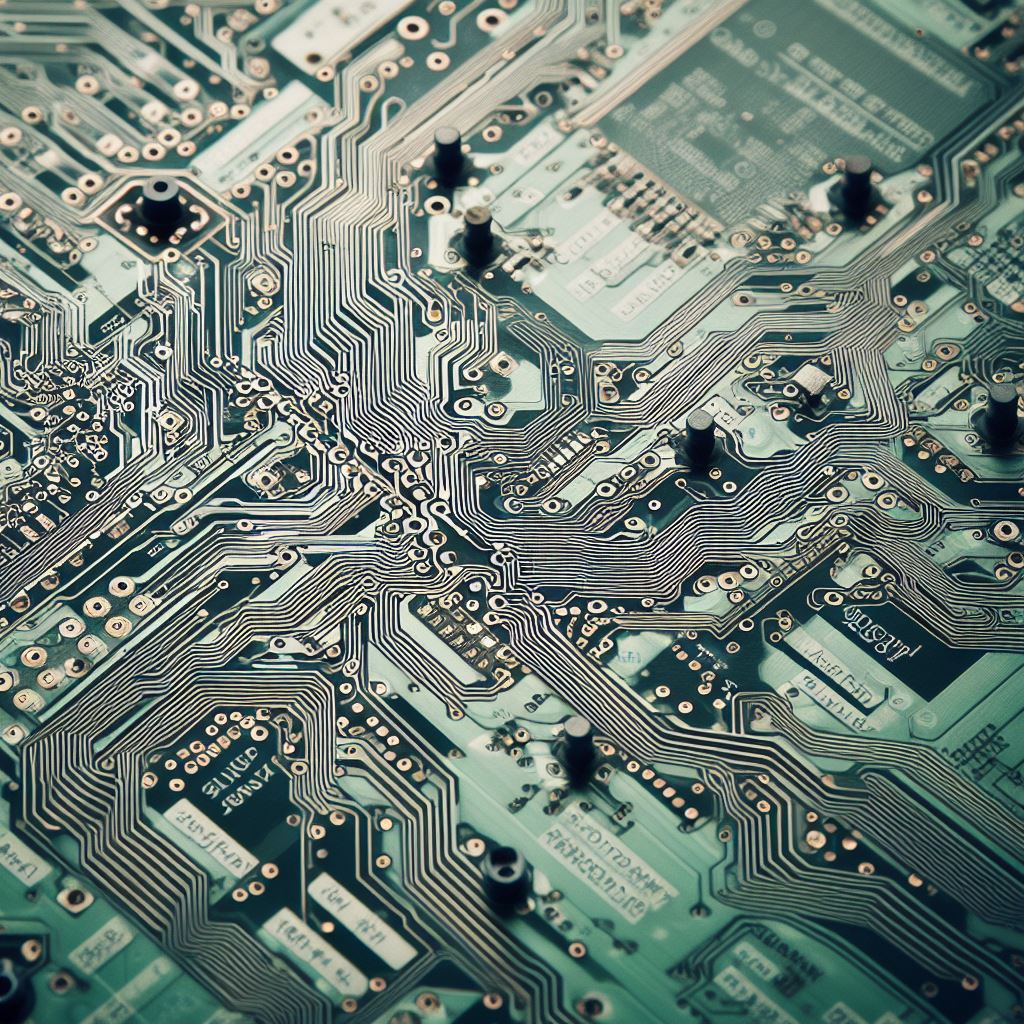
A PCB trace is a highly conductive track that is used to connect components on a printed circuit board. The traces are commonly made of copper and are fabricated during the etching process of a PCB. This article delves into the explanation of PCB trace, its vital components, and its significance to PCB design and fabrication.

Ultimate Guide to PCB Layout Design Considerations
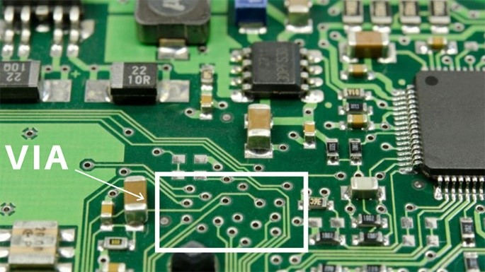
What is a Via: A Comprehensive Guide

PCB design - your 10-minute guide to create your PCB - IBE Electronics

Key Components of a PCB: Layers, Traces, and Pads Explained - Viasion PCB
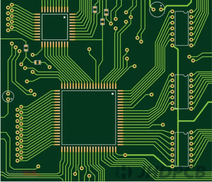
Best Guide To PCB Traces: Width, Thickness And Design Fix Recommendations - Jhdpcb
Highlight, take notes, and search in the book

PCB Design Guide to Via and Trace Currents and Temperatures
Copper Weight and Trace Width: Finding the Optimal Balance

Everything you want to know about PCB trace - IBE Electronics
Acid Trap PCB Via-Ultimate Guide On All the Things You Need to Know

Presensitized PCB: A Comprehensive Guide for Beginners – HIGH-END FPGA Distributor
The Comprehensive Guide to PCB Design